

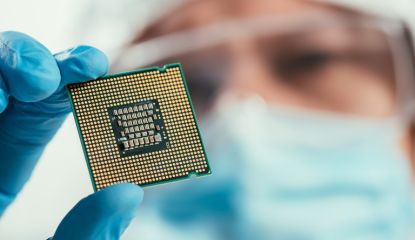
The technology is being developed as a potential alternative to conventional CMOS computing. Backed by $10.6 million from the Defence Advanced Research Projects Agency (DARPA), the method uses nanoscale mechanical strain alongside electrical signals to perform logic operations. It is led by Asif Khan, an associate professor at Georgia Tech’s School of Electrical and Computer Engineering, and his team. Traditional computer architectures have been based on the principle of moving electric charges through billions of transistors for decades.
However, artificial intelligence workloads and the increasing energy demands of data centers are pushing existing complementary metal-oxide semiconductor (CMOS) technology to its physical and thermal limits. The DARPA, as part of the Fast and Curious programme, has allocated a budget of $10.6 million to the project aiming to perform computing by using mechanical strain in semiconductors.
Logical Operations with Mechanical Strain In the project led by Associate Professor Asif Khan of the Georgia Institute of Technology Department of Electrical and Computer Engineering, a new computing method is being developed where nanometer-scale mechanical strain is used in conjunction with electrical signals. This technology, named Mechanically Enhanced Ferroic-Actuated Logic (MEFA), leverages ferroic materials that expand or contract at a microscopic level when voltage is applied. This resulting nanomechanical movement is amplified and transmitted to a nearby semiconductor channel, controlling the electron flow to enable transitions between binary logic states (1 and 0).
Emphasising that the stable representation of 1 and 0 states is more important than how information is carried during computing processes, the research team aims to combine multiple information transport methods. Much like the ferroelectric material properties highlighted in durability in future memory chips studies, the MEFA approach aims to directly reduce energy consumption by utilizing the nanomechanical behavior of ferroic structures.
The consortium, coordinated by the Georgia Institute of Technology, also includes researchers from Rice University, University of Southern California, and Space Park Foundry within Northrop Grumman. While the research team aims for their developed logic circuits to consume at least 100 times less energy compared to today’s technologies, they are prioritising making the production processes compatible with the global semiconductor infrastructure.
The plan is to transform the technology from single-component experiments into complex integrated circuits. If the project concludes successfully, power consumption can be significantly reduced while maintaining high computing speeds through the direct use of mechanical forces in logic gates.